Negative feedback or balancing feedback occurs when some function of the output of a system process or mechanism is fed back in a manner that tends to reduce the fluctuations in the output whether caused by changes in the input or by other disturbances. The first step of the demo shows how to model and simulate a linear PLL that can track a 1.

Phase Locked Loop Pll Fundamentals Analog Devices
Slide 13 Phase-Locked Loop Demodulator Slide 14 PLL Analysis Slide 15 PLL Analysis cont.

. A motor driven by square waves of current as provided by simple hall effect sensors is known as a brushless DC motor. And C hexagon containing the possible voltage vectors for SPWM. This voltage drives an external voltage-controlled oscillator VCO to increase or decrease the output.
Since an integrated circuit can hold a complete phase-locked loop building block the technique is widely used in modern electronic devices with signal frequencies from a fraction of a cycle per second up to many gigahertz. FUNCTIONAL BLOCK DIAGRAM Figure 1. A Block diagram of the SPWM generator scheme.
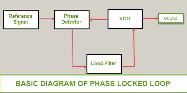
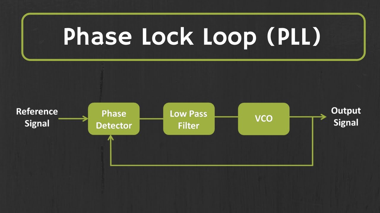
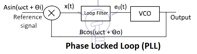
Remember me on this computer. A Phase Locked Loop PLL mainly consists of the following three blocks. 2 Slide 17 Linearized Model for PLL Slide 18 Proof PLL is a Demod for FM Slide 19 Comments on PLL Performance Slide 20 FM PLL vs.
Register Compatible with MAX3107 MAX3108 MAX3109. Phase lock clean high frequency references to 10 MHz equipment. The outputs of these two blocks are applied as inputs to the block that is present in the second.
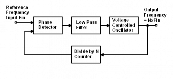
Whereas positive feedback tends to lead to instability via exponential growth oscillation or chaotic behavior negative. The block diagram of a PLL operating as a frequency synthesizer is shown in Figure 1 8. P072C Gearbox system locked in first gear P202B Short to ground in the tank heater circuit P0000 The combination appears at the end of the display of trouble codes on the display P0001 Open control wiring of the fuel supply controller.
Observe that the block diagram of an active band stop filter consists of two blocks in its first stage. 1 Slide 16 PLL Analysis cont. This chapter discusses about the block diagram of PLL and IC 565 in detail.
The block diagram of an active band stop filter is shown in the following figure. An active low pass filter and an active high pass filter. Low frequency phase-locked loops PLLs Frequency translation.
B waveforms of the modulation and carrier signals. Together with an external loop filter and a voltage controlled crystal oscillator VCXO the. Similar to the traditional two-level SPWM the amplitude of the first harmonic of the voltage supplied by the inverter is proportional to the amplitude of the modulating signal only if this latter does not.
Morgan Standard Linear Logic ABSTRACT Applications of the CD4046B phase-locked loop device such as FM demodulation FSK demodulation tone decoding frequency multiplication signal conditioning clock synchronization and frequency synthesis. The PLL is a feedback loop that wh en in lock forces. 96 MHz Fractional Digital Phase-Locked Loop FDPLL96M External Interrupt Controller EIC 16 external interrupts One Non-maskable Interrupt NMI Two-pin Serial Wire Debug SWD programming test and debugging interface Low Power Idle and Standby Sleep modes SleepWalking peripherals Peripherals 12-channel Direct Memory Access Controller DMAC.
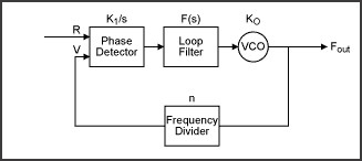
This type of motor has higher ripple. The synthesizer works in a phase-locked loop PLL where a phasefrequency detector PFD compares a fed back frequency with a divided-down version of the reference frequency Figure 1. Phase Locked Loop PLL is one of the vital blocks in linear systems.
Porter Phase Transformations in Metals and Alloys. The block diagram shows the drive electronics associated with a low voltage 12 V DC synchronous motor. These motors have a.
Enter the email address you signed up with and well email you a reset link. A Versatile Building Block for Micropower Digital and Analog Applications David K. Log in with Facebook Log in with Google.
This particular FM design uses a modern phase locked loop detector unlike the frequency discriminator or ratio detector used in earlier FM receivers. A schematic of a simple superhet broadcast FM receiver. When upper switch of a leg is on the lower switch will need to block the entire dc bus voltage and vice versa.
Hence the switches must be rated to. Niknejad PLLs and Frequency Synthesis. It consists of a reference oscillator OSC a phasefrequency detector PFD a charge pump CP a loop filter LF a voltage-controlled oscillator VCO and two frequency dividers FDs.
Oven controlled crystal oscillator OCXO frequency multipliers. P0003 On Volkswagen B VR6 and other models code. As in a single-phase square-wave inverter switches in each leg of the three-phase inverter operate in a complementary manner.
Slide 21 Laboratory Experiments for FM Slide 21 Experiment 81 Making an FM Modulator Slide. It is necessary to check the contacts on the chip with the cable and eliminate oxidation if any. Phase-locked loop controls synchronous motor speed.
Thus the switches must be rated to block the worst-case instantaneous magnitude of dc bus voltage. Here we show block diagrams for typical superheterodyne receivers for AM and FM broadcast respectively. Components include a VCO a frequency divider a phase detector PD and a loop lter.
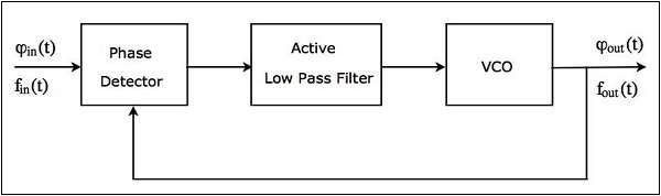
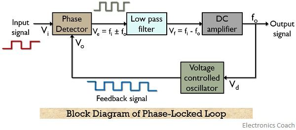
The PFDs output current pulses are filtered and integrated to generate a voltage. Block Diagram of PLL. Phase Locked Loops A PLL is a truly mixed-signal circuit involving the co.
Close Log In. Fractional Baud-Rate Generators Predivider and Phase-Locked Loop PLL Logic-Level Translation Down to 161V on the Controller and Transceiver Interfaces Ensures System Compatibility. Note that there is no AGC loop but simply uses a high-gain IF.
It is useful in communication systems such as radars satellites FMs etc. Phase Locked Loop Block Diagram ÖN Ref Div Loop Filter VCO Phase Locked Loops PLL are ubiquitous circuits used in countless communication and engineering applications.
Phase Locked Loop Operating Principle And Applications
Phase Locked Loop Ic

1 An Basic Block Diagram Of Pll Download Scientific Diagram

Describe The Basic Block Diagram Of The Phase Locked Loop Pll

Phase Locked Loops In An Ic Based Clock Distribution System Embedded Com
Activity The Phase Locked Loop Adalm2000 Analog Devices Wiki
What Is Phase Lock Loop Pll How Phase Lock Loop Works Pll Explained Youtube
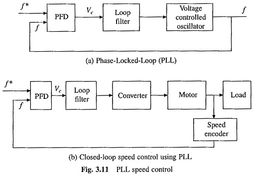
Phase Locked Loop Control Pll Speed Control Closed Loop Position Control
Glossary Definition For Pll

Phase Locked Loop Project Overview For Analog Integrated Circuits Lab Experiment
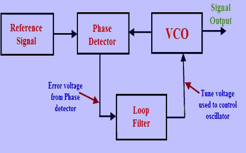
What Are Phase Locked Loops Pll Definition Block Diagram Working And Applications Of Phase Locked Loops Electronics Coach

Pll Working Phase Locked Loop Working Operation

Choose Your Pll Lock Time Measurement Edn

Phase Locked Loop Pll Fundamentals Analog Devices
Phase Locked Loop Operating Principle And Applications

Phase Locked Loops Worksheet Analog Integrated Circuits

Simulating Phase Locked Loops With Matlab
Phase Locked Loop Pll Its Operation Characteristics Application

Phase Locked Loop Tutorial Block Diagrams Electronics Circuit And Tutorials Hobby Science Projects

Posting Komentar